x86 System On Module with a custom 260-pin SODIMM pinout and plenty of I/O. 2x Intel N100 SKUs, 1x N305 SKU. N305 is new in Jan 2025 and unreviewed, plus fairly expensive vs traditional socketed CPUs.
They also have Lite and Full carrier board options with open source schematics and pinout. May not match production though, PCB has a typo in the silkscreen branding.
For firmware, they use UEFI with mainline Linux support
Proprietary firmware
Turing Pi 2 compatibility
I have a Turing Pi 2 cluster board with 260-pin SODIMM slots. Turing Machines built a Raspberry Pi CM4 adapter, could I build one for the Mu?
I got hold of this datasheet for their RK1 SOM, including a compatible pinout which we could map to the Mu.
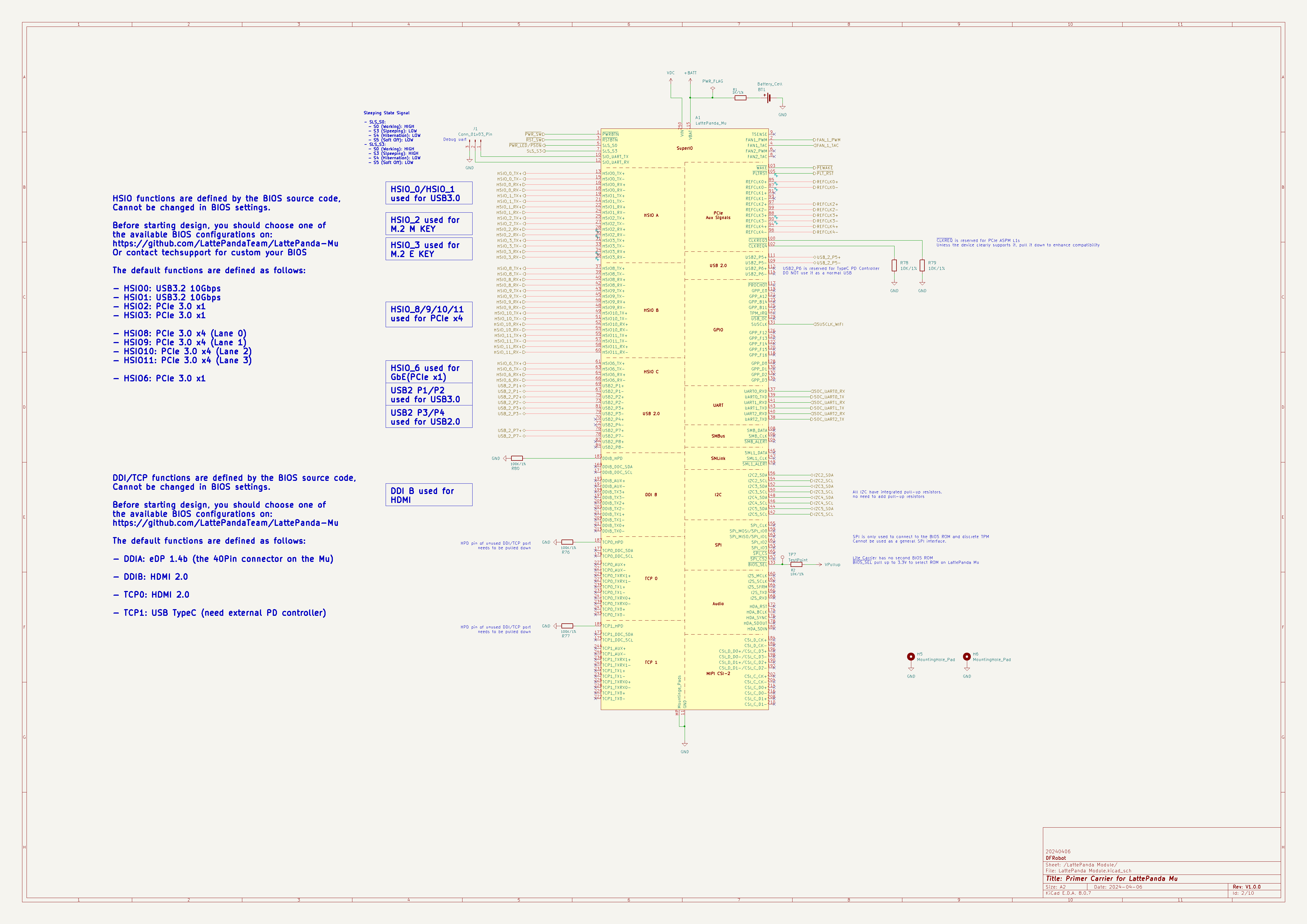
The Mu is pretty different, let’s start by mapping the essentials. The Lite carrier board schematic should help. Looks like we’ll need
- SuperIO (Super I/O) for power and debug UART
- HSIO2 for M.2 M-key (PCIe x4) ie NVMe storage
- HSIO6 for GbE (gigabit ethernet)
Those high-speed I/O (HSIO) pins are using differential signalling so we’ll need to consider EMF noise, and that’s far beyond my PCB design skills.
I was quoted 700USD and around a month on Fiverr. That’s well above my budget and I’ve only seen a few people interested in this idea, so I probably can’t recover costs. Can’t go any further unfortunately.
| RK1 Pin | Turing RK1 Function | RK1 Description | Mu Pin | Name | Type | Description | Note | RK1 Unmapped Pins |
|---|---|---|---|---|---|---|---|---|
| 237 | POWER_EN | CMOS-5.0V. Signal for module on/off: high level on, low level off. Connects to module PMIC EN0 through converter logic. POWER_EN is routed to a Schmitt trigger buffer on the module. A 45 kΩ pullup is in the PMIC. | 1 | PWRBTN# | I | Power button, with integrated pull-up | SIO PANSWH# | GND_1 |
| 2 | FAN1_PWM | O | CPU fan PWM output | SIO GP51 | GND_2 | |||
| 239 | SYS_RESET | Module Reset. Reset to the module when driven low by the carrier board. Used as carrier board supply enable when driven high by the module when module power sequence is complete. Used to ensure proper power on/off sequencing between module and carrier board supplies. | 3 | RSTBTN# | I | Reset button, with integrated pull-up | SoC SYS_RESET# | MIPI_CSI0_RX_D2N |
| 4 | FAN1_TAC | I | CPU fan tachometer input | SIO GP52 | MIPI_CSI0_RX_D0N | |||
| Add a power LED? | 5 | SLS_S0 | O | Power status, output high when S0(Working) | SIO PSON# | MIPI_CSI0_RX_D2P | ||
| 6 | TAN2_PWM | O | System fan PWM out | SIO GP36 | MIPI_CSI0_RX_D0P | |||
| Missing? | 7 | SLS_S3 | O | Power status, output high when S0(Working), S3(Sleep) | SoC GPD5 | GND_3 | ||
| 8 | FAN2_TAC | I | System fan tachometer input | SIO GP37 | GND_4 | |||
| 9 | TSENSE | I | NTC temperature sensor input | SIO TMPIN2 | MIPI_CSI0_RX_CLK1N | |||
| Debug UART | 10 | SIO_UART_TX | O | SuperIO UART transmitter | SIO JP3 | MIPI_CSI0_RX_CLK0N | ||
| Need a spare GND | 11 | GND | MIPI_CSI0_RX_CLK1P | |||||
| Debug UART | 12 | SIO_UART_RX | I | SuperIO UART receiver | SIO GP41 | MIPI_CSI0_RX_CLK0P | ||
| 13 | HSIO0_TX+ | O | Differential signal output, coupling capacitor required | GND_5 | ||||
| 14 | GND | GND_6 | ||||||
| 15 | HSIO0_TX- | O | Differential signal output, coupling capacitor required | MIPI_CSI0_RX_D3N | ||||
| 16 | HSIO0_RX+ | I | Differential signal input | MIPI_CSI0_RX_D1N | ||||
| 17 | GND | MIPI_CSI0_RX_D3P | ||||||
| 18 | HSIO0_RX- | I | Differential signal input | MIPI_CSI0_RX_D1P | ||||
| 19 | HSIO1_TX+ | O | Differential signal output, coupling capacitor required | GND_7 | ||||
| 20 | GND | GND_8 | ||||||
| 21 | HSIO1_TX- | O | Differential signal output, coupling capacitor required | MIPI_CSI1_RX_D2N | ||||
| 22 | HSIO1_RX+ | I | Differential signal input | MIPI_CSI1_RX_D0N | ||||
| 23 | GND | MIPI_CSI1_RX_D2P | ||||||
| 24 | HSIO1_RX- | I | Differential signal input | MIPI_CSI1_RX_D0P | ||||
| 25 | HSIO2_TX+ | O | Differential signal output, coupling capacitor required | GND_9 | ||||
| 26 | GND | GND_10 | ||||||
| 27 | HSIO2_TX- | O | Differential signal output, coupling capacitor required | MIPI_CSI1_RX_CLK1N | ||||
| 28 | HSIO2_RX+ | I | Differential signal input | MIPI_CSI1_RX_CLK0N | ||||
| 29 | GND | MIPI_CSI1_RX_CLK1P | ||||||
| 30 | HSIO2_RX- | I | Differential signal input | MIPI_CSI1_RX_CLK0P | ||||
| 31 | HSIO3_TX+ | O | Differential signal output, coupling capacitor required | GND_11 | ||||
| 32 | GND | GND_12 | ||||||
| 33 | HSIO3_TX- | O | Differential signal output, coupling capacitor required | MIPI_CSI1_RX_D3N | ||||
| 34 | HSIO3_RX+ | I | Differential signal input | MIPI_CSI1_RX_D1N | ||||
| 35 | GND | MIPI_CSI1_RX_D3P | ||||||
| 36 | HSIO3_RX- | I | Differential signal input | MIPI_CSI1_RX_D1P | ||||
| 37 | HSIO8_TX+ | O | Differential signal output, coupling capacitor required | GND_13 | ||||
| 38 | GND | GND_14 | ||||||
| 39 | HSIO8_TX- | O | Differential signal output, coupling capacitor required | TYPEC0_SSRX1N/DP0_TX0N | ||||
| 40 | HSIO8_RX+ | I | Differential signal input | MIPI_DPHY0_RX_D2N | ||||
| 41 | GND | TYPEC0_SSRX1P/DP0_TX0P | ||||||
| 42 | HSIO8_RX- | I | Differential signal input | MIPI_DPHY0_RX_D2P | ||||
| 43 | HSIO9_TX+ | O | Differential signal output, coupling capacitor required | GND_15 | ||||
| 44 | GND | GND_16 | ||||||
| 45 | HSIO9_TX- | O | Differential signal output, coupling capacitor required | TYPEC0_SSTX1N/DP0_TX1N | ||||
| 46 | HSIO9_RX+ | I | Differential signal input | MIPI_DPHY0_RX_D0N | ||||
| 47 | GND | TYPEC0_SSTX1P/DP0_TX1P | ||||||
| 48 | HSIO9_RX- | I | Differential signal input | MIPI_DPHY0_RX_D0P | ||||
| 49 | HSIO10_TX+ | O | Differential signal output, coupling capacitor required | GND_17 | ||||
| 50 | GND | GND_18 | ||||||
| 51 | HSIO10_TX- | O | Differential signal output, coupling capacitor required | TYPEC0_SSRX2N/DP0_TX2N | ||||
| 52 | HSIO10_RX+ | I | Differential signal input | MIPI_DPHY0_RX_CLKN | ||||
| 53 | GND | TYPEC0_SSRX2P/DP0_TX2P | ||||||
| 54 | HSIO10_RX- | I | Differential signal input | MIPI_DPHY0_RX_CLKP | ||||
| 55 | HSIO11_TX+ | O | Differential signal output, coupling capacitor required | GND_19 | ||||
| 56 | GND | GND_20 | ||||||
| 57 | HSIO11_TX- | O | Differential signal output, coupling capacitor required | TYPEC0_SSTX2N/DP0_TX3N | ||||
| 58 | HSIO11_RX+ | I | Differential signal input | MIPI_DPHY0_RX_D1N | ||||
| 59 | GND | TYPEC0_SSTX2P/DP0_TX3P | ||||||
| 60 | HSIO11_RX- | I | Differential signal input | MIPI_DPHY0_RX_D1P | ||||
| 61 | HSIO6_TX+ | O | Differential signal output, coupling capacitor required | GND_21 | ||||
| 62 | GND | GND_22 | ||||||
| 63 | HSIO6_TX- | O | Differential signal output, coupling capacitor required | HDMI_TX2_N | ||||
| 64 | HSIO6_RX+ | I | Differential signal input | MIPI_DPHY0_RX_D3N | ||||
| 65 | GND | HDMI_TX2_P | ||||||
| 66 | HSIO6_RX- | I | Differential signal input | MIPI_DPHY0_RX_D3P | ||||
| 67 | USB2_P1- | I/O | USB 2.0 differential signal | GND_23 | ||||
| 68 | GND | GND_24 | ||||||
| 69 | USB2_P1+ | I/O | USB 2.0 differential signal | HDMI_TX1_N | ||||
| 70 | USB2_P4 | I/O | USB 2.0 differential signal | MIPI_DPHY0_TX_D0N | ||||
| 71 | GND | HDMI_TX1_P | ||||||
| 72 | USB2_N4 | I/O | USB 2.0 differential signal | MIPI_DPHY0_TX_D0P | ||||
| 73 | USB2_P2- | I/O | USB 2.0 differential signal | GND_25 | ||||
| 74 | GND | GND_26 | ||||||
| 75 | USB2_P2+ | I/O | USB 2.0 differential signal | HDMI_TX0_N | ||||
| 76 | USB2_P7 | I/O | USB 2.0 differential signal | MIPI_DPHY0_TX_CLKN | ||||
| 77 | GND | HDMI_TX0_P | ||||||
| 78 | USB2_N7 | I/O | USB 2.0 differential signal | MIPI_DPHY0_TX_CLKP | ||||
| 79 | USB2_P3- | I/O | USB 2.0 differential signal | GND_27 | ||||
| 80 | GND | GND_28 | ||||||
| 81 | USB2_P3+ | I/O | USB 2.0 differential signal | HDMI_TXC_N | ||||
| 82 | USB2_P8 | I/O | USB 2.0 differential signal | MIPI_DPHY0_TX_D1N | ||||
| 83 | GND | HDMI_TXC_P | ||||||
| 84 | USB2_N8 | I/O | USB 2.0 differential signal | MIPI_DPHY0_TX_D1P | ||||
| 85 | REFCLK0+ | O | PCIe reference clock | GND_29 | ||||
| 86 | GND | GND_30 | ||||||
| 87 | REFCLK0- | O | PCIe reference clock | GPIO3_C1 | ||||
| 88 | REFCLK3+ | O | PCIe reference clock | DP0_HPDIN_M1 | ||||
| 89 | GND | SPI0_MOSIM2 | ||||||
| 90 | REFCLK3- | O | PCIe reference clock | TYPEC0_SBU2/DP0_AUXN | ||||
| 91 | REFCLK1+ | O | PCIe reference clock | SPI0_CLK_M2 | ||||
| 92 | GND | TYPEC0_SBU1/DP0_AUXP | ||||||
| 93 | REFCLK1- | O | PCIe reference clock | SPI0_MISO_M2 | ||||
| 94 | REFCLK4+ | O | PCIe reference clock | HDMI_CEC | ||||
| 95 | GND | SPI0_CS0_M2 | ||||||
| 96 | REFCLK4- | O | PCIe reference clock | HDMI_HPD | ||||
| 97 | REFCLK2+ | O | PCIe reference clock | SPI0_CS1_M2 | ||||
| 98 | GND | HDMI_DDC_SDA_POL | ||||||
| 99 | REFCLK2- | O | PCIe reference clock | |||||
| 100 | PCIECLK_REQ3# | I | REFCLK3 clock request function | SoC GPP_D8 | HDMI_DDC_SCL_POL | |||
| 101 | GND | |||||||
| 102 | PCIECLK_REQ4# | I | REFCLK4 clock request function | SoC GPP_H19 | GND_31 | |||
| 103 | WAKE# | I | Wake Mu when pull-down | SoC WAKE# | UART6_RTSn_M0 | |||
| 104 | SMB_ALERT# | I | SMBus alert interrupt | SoC GPP_C2 | SPI2_MOSI_M1 | |||
| 105 | PLTRST# | O | Platform reset signal | SoC GPP_B13 | UART6_CTSn_M0 | |||
| 106 | SMB_CLK | O | SMBus clock | SoC GPP_C0 | SPI2_CLK_M1 | |||
| 107 | GND | GND_32 | ||||||
| 108 | SMB_DATA | I/O | SMBus data | SoC GPP_C1 | SPI2_MISO_M1 | |||
| 109 | USB2_P5- | I/O | USB 2.0 differential signal | USB0_OTG_D_N | ||||
| 110 | GND | SPI2_CS0_M1 | ||||||
| 111 | USB2_P5+ | I/O | USB 2.0 differential signal | USB0_OTG_D_P | ||||
| 112 | USB2_P6 | I/O | USB 2.0 differential signal | SPI2_CS1_M1 | ||||
| 113 | GND | GND_33 | ||||||
| 114 | USB2_N6 | I/O | USB 2.0 differential signal | MIPI_CAM3_PDN_L | ||||
| 235 | RTC_BAT_IN | Bidir 1.65V-5.5V | 115 | VBAT | RTC battery input | SoC VCCRTC | USB1_OTG_D_N | |
| 116 | GND | MIPI_CAM3_CLKOUT | ||||||
| 117 | PROCHOT# | I | Overheat protect when pull-down | SoC PROCHOT# | USB1_OTG_D_P | |||
| 118 | GPP_F16 | I/O | GPIO, functions defined by BIOS | GPIO3_C6 | ||||
| 119 | GPP_E0 | I/O | GPIO, functions defined by BIOS | GND_34 | ||||
| 120 | GPP_F15 | I/O | GPIO, functions defined by BIOS | MIPI_CAM4_PDN_L | ||||
| 121 | GPP_A12 | I/O | GPIO, functions defined by BIOS | USB2_HOST0_D_N | ||||
| 122 | GPP_F14 | I/O | GPIO, functions defined by BIOS | MIPI_CAM4_CLKOUT | ||||
| 123 | GPP_B14 | I/O | GPIO, functions defined by BIOS | USB2_HOST0_D_P | ||||
| 124 | GPP_F13 | I/O | GPIO, functions defined by BIOS | GPIO3_C7 | ||||
| 125 | GPP_B11 | I/O | GPIO, functions defined by BIOS | GND_35 | ||||
| 126 | GPP_F12 | I/O | GPIO, functions defined by BIOS | GPIO3_D0/PWM8_M2 | ||||
| 127 | TPM_IRQ | I | discrete TPM interrupt | SoC GPP_B4 | GPIO3_D1/PWM9_M2 | |||
| 128 | GPP_D0 | I/O | GPIO, functions defined by BIOS | GPIO3_D2 | ||||
| 129 | USB_OC# | I | USB over current signal | SoC GPP_A16 | GND_36 | |||
| 130 | GPP_D1 | I/O | GPIO, functions defined by BIOS | GPIO3_D4 | ||||
| 131 | SUSCLK | O | 32.768kHz clock output | SoC GPD8 | PCIE30_PORT0_RX0N | |||
| 132 | GPP_D2 | I/O | GPIO, functions defined by BIOS | GND_37 | ||||
| 133 | BIOS_SEL# | I | BIOS select: pull-up: integrated ROM; pull-down: carrier ROM | PCIE30_PORT0_RX0P | ||||
| 134 | GPP_D3 | I/O | GPIO, functions defined by BIOS | PCIE30_PORT0_TX0N | ||||
| 135 | GND | GND_38 | ||||||
| 136 | GND | PCIE30_PORT0_TX0P | ||||||
| 101 | UART6_RXD_M0 | 137 | UART0_RXD | I | SoC UART0 receiver | SoC GPP_H10 | PCIE30_PORT0_RX1N | |
| 236 | UART2_TXD_M0_DEBUG | 138 | SOC_UART2_TXD | O | SoC UART2 transmitter | SoC GPP_F2 | GND_39 | |
| 99 | UART6_TXD_M0 | 139 | UART0_TXD | O | SoC UART0 transmitter | SoC GPP_H11 | PCIE30_PORT0_RX1P | |
| 238 | UART2_RXD_M0_DEBUG | 140 | SOC_UART2_RXD | I | SoC UART2 receiver | SoC GPP_F1 | PCIE30_PORT0_TX1N | |
| 205 | UART9_RX_M0_BT | 141 | UART1_RXD | I | SoC UART1 receiver | SoC GPP_D17 | GND_40 | |
| 142 | I2C5_SCL | O | I2C5 clock | SoC GPP_B17 | PCIE30_PORT0_TX1P | |||
| 203 | UART9_TX_M0_BT | 143 | UART1_TXD | O | SoC UART1 transmitter | SoC GPP_D18 | CAN2_RX_M0 | |
| 144 | I2C5_SDA | I/O | I2C5 data | SoC GPP_B16 | GND_41 | |||
| 145 | SML1_DATA | I/O | SMLink1 data | SoC GPP_C7 | CAN2_TX_M0 | |||
| 146 | I2C4_SCL | O | I2C4 clock | SoC GPP_H9 | GND_42 | |||
| 147 | SML1_CLK | O | SMLink1 clock | SoC GPP_C6 | GND_43 | |||
| 148 | I2C4_SDA | I/O | I2C4 data | SoC GPP_H8 | PCIE30_PORT1_TX2N | |||
| 149 | SML1_ALERT# | I | SMLink1 alert | SoC GPP_B23 | PCIE30_PORT1_RX2N | |||
| 150 | I2C3_SCL | O | I2C3 clock | SoC GPP_B8 | PCIE30_PORT1_TX2P | |||
| 151 | GND | PCIE30_PORT1_RX2P | ||||||
| 152 | I2C3_SDA | I/O | I2C3 data | SoC GPP_B7 | GND_44 | |||
| 153 | SPI_IO3 | I/O | SPI interface, BIOS and dTPM specific | GND_45 | ||||
| 154 | I2C2_SCL | O | I2C2 clock | SoC GPP_B6 | PCIE30_PORT1_TX3N | |||
| 155 | SPI_CLK | O | SPI interface, BIOS and dTPM specific | PCIE30_PORT1_RX3N | ||||
| 156 | I2C2_SDA | I/O | I2C2 data | SoC GPP_B5 | PCIE30_PORT1_TX3P | |||
| 157 | SPI_CS2# | O | SPI chip select, dTPM specific | PCIE30_PORT1_RX3P | ||||
| 158 | GND | GND_46 | ||||||
| 159 | SPI_MOSI/SPI_IO0 | I/O | SPI interface, BIOS and dTPM specific | GND_47 | ||||
| 160 | I2S_MCLK | O | I2S main clock | SoC GPP_D19 | PCIE30_REFCLKN_SLOT | |||
| 161 | SPI_IO2 | I/O | SPI interface, BIOS and dTPM specific | TYPEC1_SSRX1N | ||||
| 162 | I2S_SCLK | O | I2S bit clock | SoC GPP_S0 | PCIE30_REFCLKP_SLOT | |||
| 163 | SPI_MISO/SPI_IO1 | I/O | SPI interface, BIOS and dTPM specific | TYPEC1_SSRX1P | ||||
| 164 | I2S_SFRM | O | I2S word clock | SoC GPP_S1 | GND_48 | |||
| 165 | SPI_CS# | O | SPI chip select, BIOS ROM specific | GND_49 | ||||
| 166 | I2S_TXD | O | I2S serial data transmitter | SoC GPP_S2 | TYPEC1_SSTX1N | |||
| 167 | GND | PCIE20_2_RXN | ||||||
| 168 | I2S_RXD | I | I2S serial data receiver | SoC GPP_S3 | TYPEC1_SSTX1P | |||
| 169 | DDIB_DDC_SDA | I/O | DDIB HDMI display data channel data | SoC GPP_H17 | PCIE20_2_RXP | |||
| 170 | GND | GND_50 | ||||||
| 171 | DDIB_DDC_SCL | O | DDIB HDMI display data channel clock | SoC GPP_H15 | GND_51 | |||
| 172 | HDA_RST | O | HD Audio reset | SoC GPP_R4 | PCIE20_2_TXN | |||
| 173 | TCP1_DDC_SDA | I/O | TCP1 HDMI display data channel data | SoC GPP_E21 | PCIE20_2_REFCLKN | |||
| 174 | HDA_BCLK | O | HD Audio bit clock | SoC GPP_R0 | PCIE20_2_TXP | |||
| 175 | TCP1_DDC_SCL | O | TCP1 HDMI display data channel clock | SoC GPP_E20 | PCIE20_2_REFCLKP | |||
| 176 | HDA_SYNC | O | HD Audio sync | SoC GPP_R1 | GND_52 | |||
| 177 | TCP0_DDC_SDA | I/O | TCP0 HDMI display data channel data | SoC GPP_E19 | GND_53 | |||
| 178 | HDA_SDOUT | O | HD Audio serial data out | SoC GPP_R2 | NC | |||
| 179 | TCP0_DDC_SCL | O | TCP0 HDMI display data channel clock | SoC GPP_E18 | PCIE30X4/ PCIEX1_1_WAKE_M1 | |||
| 180 | HDA_SDIN | I | HD Audio serial data in | SoC GPP_R3 | PCIE30X4_CLKREQ_M1 | |||
| 181 | GND | PCIE30X4_RST_M1 | ||||||
| 182 | GND | PCIEX1_1_CLKREQ_M1 | ||||||
| Ground this | 183 | DDIB_HPD | I | DDIB hot plug detect | SoC GPP_A18 | PCIEX1_1_RST_M1 | ||
| 184 | CSI_D_CK+ | I | MIPI CSI-2 Port D Clock | GBE_MDI0_N | ||||
| Ground this | 185 | TCP1_HPD | I | TCP1 hot plug detect | SoC GPP_A20 | I2C5_SCL_M3 | ||
| 186 | CSI_D_CK- | I | MIPI CSI-2 Port D Clock | GBE_MDI0_P | ||||
| Ground this | 187 | TCP0_HPD | I | TCP0 hot plug detect | SoC GPP_A19 | I2C5_SDA_M3 | ||
| 188 | GND | GBE_LED_ACT | ||||||
| 189 | GND | I2C4_SCL_M1 | ||||||
| 190 | CSI_D_D1+ | I | MIPI CSI-2 Port D Data Lane 1 | GBE_MDI1_N | ||||
| 191 | DDIB_AUX- | I/O | DDIB DP Auxiliary channel | I2C4_SDA_M1 | ||||
| 192 | CSI_D_D1- | I | MIPI CSI-2 Port D Data Lane 1 | GBE_MDI1_P | ||||
| 193 | DDIB_AUX+ | I/O | DDIB DP Auxiliary channel | I2S0_SDO0 | ||||
| 194 | GND | GBE_LED_LINK | ||||||
| 195 | GND | I2S0_SDI0 | ||||||
| 196 | CSI_D_D0+ | I | MIPI CSI-2 Port D Data Lane 0 | GBE_MDI2_N | ||||
| 197 | DDIB_TX3- | O | DDIB DP Lane 3/HDMI TMDS Clock | I2S0_LRCK | ||||
| 198 | CSI_D_D0- | I | MIPI CSI-2 Port D Data Lane 0 | GBE_MDI2_P | ||||
| 199 | DDIB_TX3+ | O | DDIB DP Lane 3/HDMI TMDS Clock | I2S0_SCLK | ||||
| 200 | GND | GND_54 | ||||||
| 201 | GND | GND_55 | ||||||
| 202 | CSI_C_CK+ | I | MIPI CSI-2 Port C Clock | GBE_MDI3_N | ||||
| 203 | DDIB_TX2- | O | DDIB DP Lane 2/HDMI TMDS Data0 | |||||
| 204 | CSI_C_CK- | I | MIPI CSI-2 Port C Clock | GBE_MDI3_P | ||||
| 205 | DDIB_TX2+ | O | DDIB DP Lane 2/HDMI TMDS Data0 | |||||
| 206 | GND | GPIO3_D3/PWM10_M2 | ||||||
| 207 | GND | UART9_RTSn_M0_BT | ||||||
| 208 | CSI_C_D1+ | I | MIPI CSI-2 Port C Data Lane 1 | SDMMC_DET/GPIO0_A4 | ||||
| 209 | DDIB_TX1- | O | DDIB DP Lane 1/HDMI TMDS Data1 | UART9_CTSn_M0_BT | ||||
| 210 | CSI_C_D1- | I | MIPI CSI-2 Port C Data Lane 1 | CLK_32K_OUT | ||||
| 211 | DDIB_TX1+ | O | DDIB DP Lane 1/HDMI TMDS Data1 | GPIO4_B1 | ||||
| 212 | GND | GPIO4_B3 | ||||||
| 213 | GND | I2C3_SCL_M0 | ||||||
| 214 | CSI_C_D0+ | I | MIPI CSI-2 Port C Data Lane 0 | FORCE_RECOVERY | ||||
| 215 | DDIB_TX0- | O | DDIB DP Lane 0/HDMI TMDS Data2 | I2C3_SDA_M0 | ||||
| 216 | CSI_C_D0- | I | MIPI CSI-2 Port C Data Lane 0 | GPIO1_A6 | ||||
| 217 | DDIB_TX0+ | O | DDIB DP Lane 0/HDMI TMDS Data2 | GND_56 | ||||
| 218 | GND | GPIO1_A4 | ||||||
| 219 | GND | SDMMC_DAT0 | ||||||
| 220 | TCP1_TXP0 | O | TCP1 DP Lane 0/HDMI TMDS Data2 | I2S2_SDO_M0_BT | ||||
| 221 | TCP0_AUX- | I/O | TCP0 DP Auxiliary channel | SDMMC_DAT1 | ||||
| 222 | TCP1_TXN0 | O | TCP1 DP Lane 0/HDMI TMDS Data2 | I2S2_SDI_M0_BT | ||||
| 223 | TCP0_AUX+ | I/O | TCP0 DP Auxiliary channel | SDMMC_DAT2 | ||||
| 224 | GND | I2S2_LRCK_M0_BT | ||||||
| 225 | GND | SDMMC_DAT3 | ||||||
| 226 | TCP1_TXRXP0 | O | TCP1 DP Lane 1/HDMI TMDS Data1 | I2S2_SCLK_M0_BT | ||||
| 227 | TCP0_TXRX1- | O | TCP0 DP Lane 3/HDMI TMDS Clock | SDMMC_CMD | ||||
| 228 | TCP1_TXRXN0 | O | TCP1 DP Lane 1/HDMI TMDS Data1 | GPIO1_A3/PWM1_M2 | ||||
| 229 | TCP0_TXRX1+ | O | TCP0 DP Lane 3/HDMI TMDS Clock | SDMMC_CLK | ||||
| 230 | GND | GPIO1_A2/PWM0_M2 | ||||||
| 231 | GND | GND_57 | ||||||
| 232 | TCP1_TXP1 | O | TCP1 DP Lane 2/HDMI TMDS Data0 | I2C7_SCL_M0_CODEC | ||||
| 233 | TCP0_TX1- | O | TCP0 DP Lane 2/HDMI TMDS Data0 | NC | ||||
| 234 | TCP1_TXN1 | O | TCP1 DP Lane 2/HDMI TMDS Data0 | I2C7_SDA_M0_CODEC | ||||
| 235 | TCP0_TX1+ | O | TCP0 DP Lane 2/HDMI TMDS Data0 | |||||
| 236 | GND | |||||||
| 237 | GND | |||||||
| 238 | TCP1_TXRXP1 | O | TCP1 DP Lane 3/HDMI TMDS Clock | |||||
| 239 | TCP0_TXRX0- | O | TCP0 DP Lane 1/HDMI TMDS Data1 | |||||
| 240 | TCP1_TXRXN1 | O | TCP1 DP Lane 3/HDMI TMDS Clock | NC | ||||
| 241 | TCP0_TXRX0+ | O | TCP0 DP Lane 1/HDMI TMDS Data1 | GND_58 | ||||
| 242 | GND | GND_59 | ||||||
| 243 | GND | GND_60 | ||||||
| 244 | TCP1_AUX_P | I/O | TCP1 DP Auxiliary channel | GND_61 | ||||
| 245 | TCP0_TX0- | O | TCP0 DP Lane 0/HDMI TMDS Data2 | GND_62 | ||||
| 246 | TCP1_AUX_N | I/O | TCP1 DP Auxiliary channel | GND_63 | ||||
| 247 | TCP0_TX0+ | O | TCP0 DP Lane 0/HDMI TMDS Data2 | GND_64 | ||||
| 248 | GND | GND_65 | ||||||
| 249 | GND | GND_66 | ||||||
| 250 | VDC | Main power input 9~20V | GND_67 | |||||
| 251 | VDD_IN_1 | 251 | VIN | Main power input 9~20V | ||||
| 252 | VDD_IN_2 | 252 | VDC | Main power input 9~20V | ||||
| 253 | VDD_IN_3 | 253 | VIN | Main power input 9~20V | ||||
| 254 | VDD_IN_4 | 254 | VDC | Main power input 9~20V | ||||
| 255 | VDD_IN_5 | 255 | VIN | Main power input 9~20V | ||||
| 256 | VDD_IN_6 | 256 | VDC | Main power input 9~20V | ||||
| 257 | VDD_IN_7 | 257 | VIN | Main power input 9~20V | ||||
| 258 | VDD_IN_8 | 258 | VDC | Main power input 9~20V | ||||
| 259 | VDD_IN_9 | 259 | VIN | Main power input 9~20V | ||||
| 260 | NC | 260 | VDC | Main power input 9~20V |